
Common-mode current is unwanted current that flows in the same direction on two or more conductors, returning through a shared path such as a ground plane, chassis, or earth. Because the fields from each conductor reinforce one another, common-mode current radiates far more strongly than ordinary signal current, which is why it is a frequent cause of radiated and conducted emissions failures.
If you look up most EMC guides on the internet, they will mention common-mode noise, which originates from common-mode current. Common-mode noise gets a bad rap at high frequencies because the electromagnetic fields around paired conductors interfere constructively, causing strong emissions at relatively low currents. This is why FCC rules and other regulations limit common-mode noise, e.g., on cabling, to very low levels. This has an upstream effect on mode conversion in high-speed interfaces and unintentional capacitive coupling in many other cases.
In order to overcome an EMC failure caused by excess common-mode noise, the designer or test engineer needs to do three things:
- Locate the source of common-mode noise and eliminate it.
- Filter the common-mode noise before it can radiate strongly.
- Use shielding to suppress emissions from common-mode noise.
This article will focus on the first item in the list, specifically focusing on two common areas where common-mode noise arises: heatsinks and the device enclosure.
How does common-mode current couple to a metallized enclosure?
A metallized enclosure picks up common-mode current when parasitic capacitance between the PCB and the enclosure lets high-frequency current flow across that gap, then return to the board through the chassis ground connection. The result is a current loop that can radiate.
Common-mode currents arising through metallized enclosures are one of the easier ways to visualize how this source of EMI occurs. When this occurs, current appears on groups of signal lines in a PCB. This noise can interfere with certain circuits and might cause enough radiation from the PCB to be noticed during emissions testing. If the currents make their way onto a cable, they can radiate very strongly and will be a major factor in passing radiated emissions tests. Furthermore, if the cable is a power cable or connects to some other system, there is a chance that the common-mode noise will violate conducted emissions limits.
When traveling through the enclosure, the noise originates through parasitic capacitance between the PCB and the enclosure. This creates a potential difference across the enclosure that allows some current to flow, as shown in the image below.
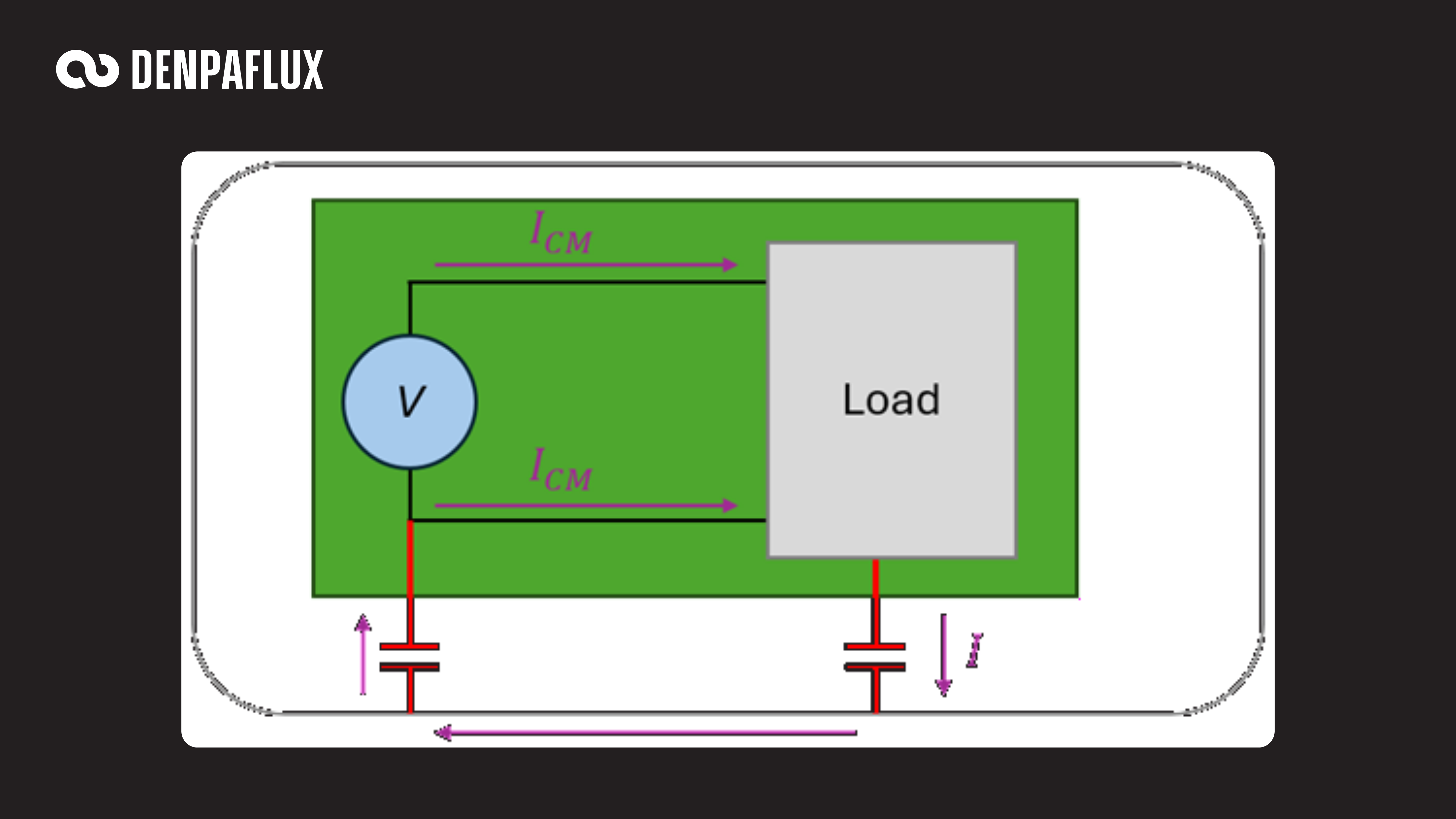 Common-mode current path from a PCB coupling to a metallized enclosure.
By coupling to an enclosure through unintended capacitance, the current can circulate back onto the PCB via a chassis ground connection. Because this current path includes capacitance, the noise tends to occur at high frequencies, generally in the high-MHz range or higher.
This is closely related to how chassis and earth grounds can end up carrying current they were never meant to. For the grounding side of that problem, see our guide on grounding mistakes in high voltage converter layouts.
How do heatsinks generate common-mode current?
Heatsinks generate common-mode current when parasitic capacitance couples a fast-switching node to the heatsink, and further capacitance from the heatsink to the enclosure completes the loop. Because the heatsink is a large grounded conductor sitting close to hot switching components, it is an efficient antenna for this displacement current.
The enclosure is a common large piece of metal that can conduct currents, but there is another category of conductor that can participate in generating common-mode currents through an enclosure: heatsinks. Depending on how heatsinks are mounted or arranged near switching circuits and the enclosure, parasitic capacitance can allow a displacement current to propagate on the heatsink.
The resulting path for a heatsink (which is typically grounded) and the surrounding enclosure would look like the path shown below:
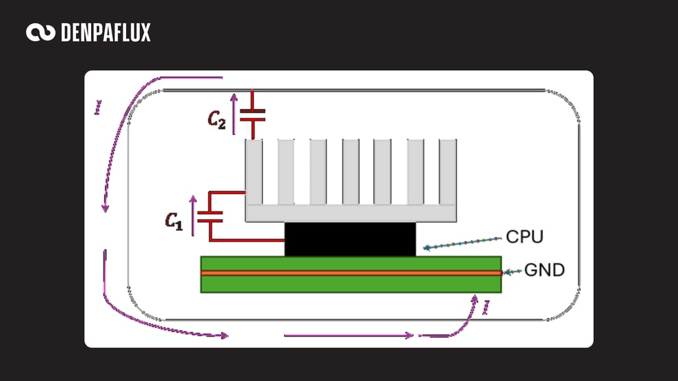 Example common-mode noise current path through a heatsink with a digital processor.
The capacitance from the heat sink to the enclosure (C2) can be much larger than the CPU-to-heatsink capacitance (C1) due to the physical size of the conductors involved. That connection completes the current loop for common-mode noise, and it is possible for the common-mode noise to radiate away from the PCBA.
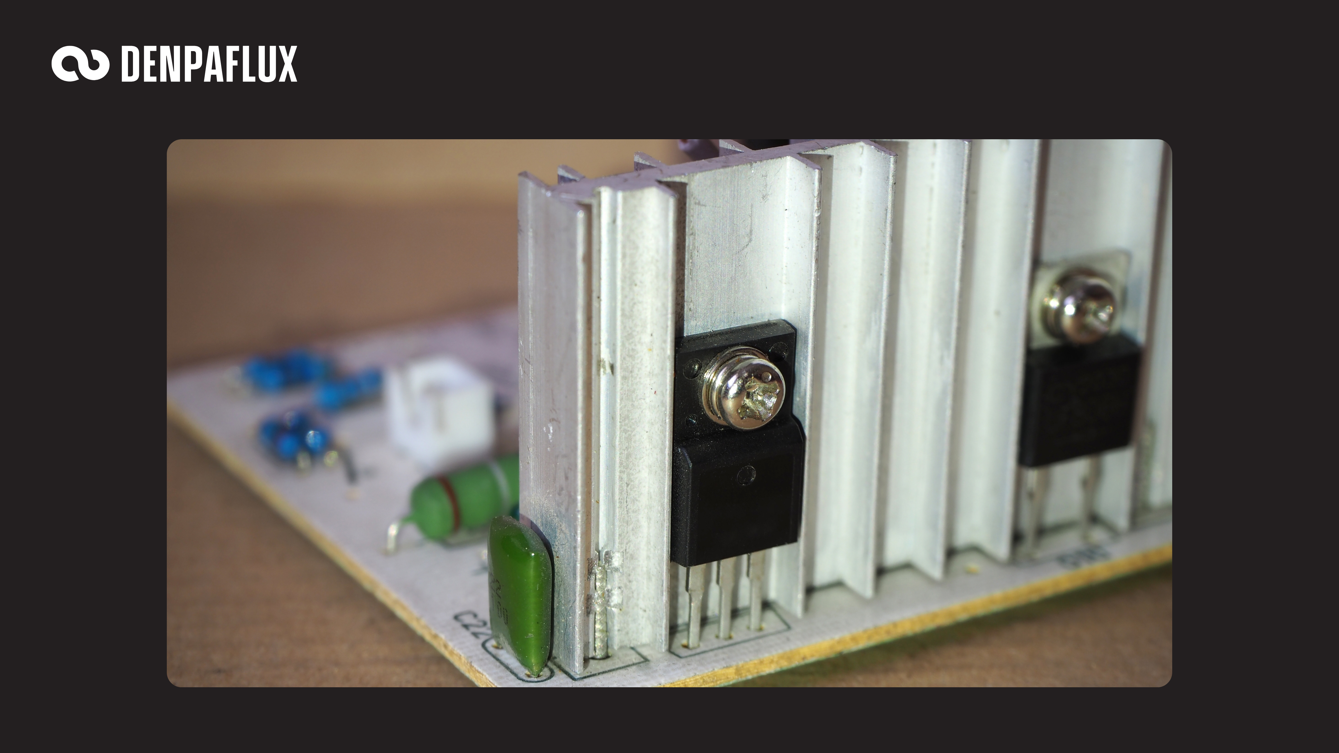
While we might expect that the most common instance is common-mode noise on a large processor heatsink, this is not strictly true. Screw-mount heatsinks on TO packages for FETs are also a common instance where common-mode currents can originate. In that case, it is even possible to gang multiple MOSFETs onto a shared heatsink, potentially creating multiple common-mode current sources coupling to a single conductor.
What can you do about common-mode noise?
To reduce common-mode noise, first find the fast-switching node that is driving it, then reduce the coupling between that node and the large conductor picking it up. In practice that means increasing distance, shrinking the coupling area, adding bonding or grounding points, and slowing the driving signal's edge rate.
The next question is: what is the source of the charge or field that couples across any parasitic capacitance? Technically, it could be anything with a high dV/dt value, i.e., switching signals, but it is not strictly limited to digital signals. The dV/dt value and the parasitic capacitance C tell us the current induced in the nearby conductor:
I = C(dV/dt)
This hints at the idea that, in order to locate the source of common-mode coupling, the largest nearby conductor may be to blame. This is because large conductor surfaces might create large capacitance to an element on the PCB, such as a copper pour used in a switching node. So to help reduce emissions from these common EMI sources, we might do the following:
- Move coupled traces/nodes farther from the enclosure/heatsink
- Reduce the size of the coupling area
- Add bonding points (for enclosures) or grounding points (for heatsinks)
- Reduce driving signal slew rates
Slew-rate control and stackup choices are also central to reducing emissions without adding a shielding can. For those techniques, see our guide on shieldless EMC strategies. And because a fast switch node is the root driver here, the same ringing that feeds common-mode noise is what an RC snubber or RCD clamp is designed to damp.
Common-mode noise that starts and ends in the PCB is not guaranteed to cause a radiated emissions failure, as the GND plane creates an image current which shields the emissions from the external environment. However, the common-mode noise that leaves the device through a cable is much more of a problem. Due to the constructively interfering electromagnetic field from each conductor carrying common-mode noise, the radiation from common-mode noise is much stronger than radiation from uncorrelated noise currents on the same set of conductors.
How do you stop common-mode current on a cable?
When common-mode current reaches a cable, the fix is to add impedance to the common-mode path or to give it a controlled return. The common options are a common-mode choke or filter at the connector, a ferrite on the cable, a shielded cable with a carefully chosen shield ground, or a discrete filter circuit.
When cables are involved, there are several options:
- Place a common-mode EMI filter IC or choke at the connector
- Place a ferrite choke on the cable at the output
- Use a shielded cable, but you should experiment with the shield ground connection
- Use a filter circuit designed from discrete components
Frequently asked questions
To help identify potential EMI sources in your PCB layout, look to DENPAFLUX for fast evaluation and qualification of your design. We review your layout against the industry standards and regional regulations that apply to your product, then return a report that pinpoints likely EMI sources with concrete recommendations for fixing them.
How much we take on is your call. Some teams want an independent expert review to validate their direction. Others want us validating every step as they implement, with formal sign-off before each test. And some want EMC handled end to end so they can stay focused on the product. Whichever fits where you are, the same team and the same diagnostic depth sits behind your project.
.png?width=352&name=Why%20_70%25%20of%20HV%20Products%20Fail%20EMC%20the%20First%20Time%20(2).png)
.png?width=352&name=EMC%20basics%20for%20SiC_GaN%20switching%20-%20What%20changed%20vs.%20IGBT%20(2).png)