
%20(1).webp?width=4480&height=2520&name=Top%204%20Grounding%20Mistakes%20in%20High%20Voltage%20Converter%20Layouts%20(2)%20(1).webp)
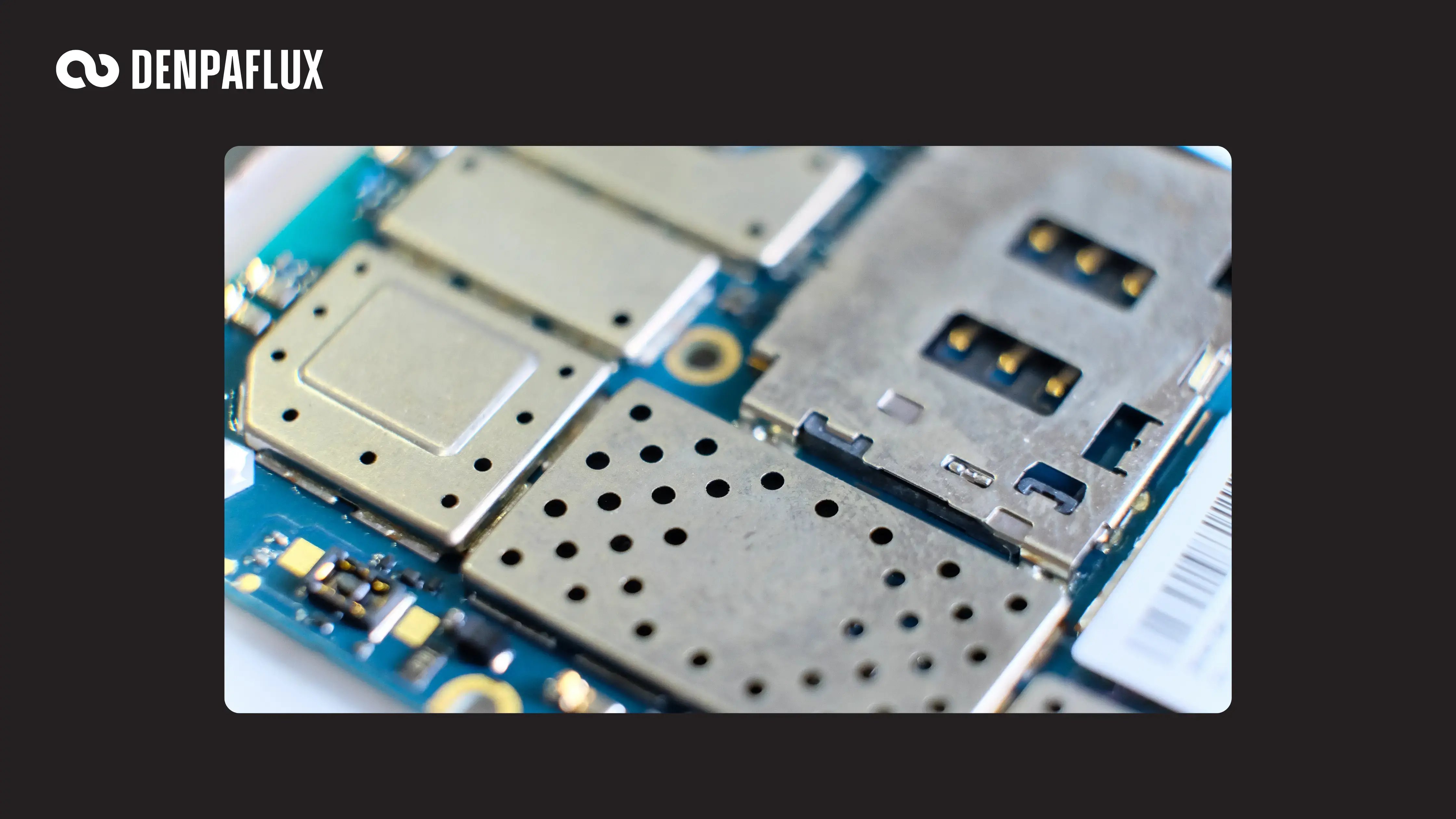
When I first started working on PCBs, I would often see photographs of devices with metal shielding cans or cages in strategic portions of the PCB layout. I would also see this in some older electronics that I would tear down, such as old smartphones. These experiences created the perception that shielding cages on the PCB were mandatory for containing noise. I later learned that this was not the case.
There are many instances where board-level shielding is not mandatory, but it is found that the shielding provides a quick path to EMC compliance during testing. In some cases, designers will repeatedly fail pre-compliance, and due to schedule pressure, they incorporate board-level shielding as a last resort. This happens in all sorts of designs, not just old smartphones.
So before you start throwing metal shielding cages on your PCB, consider these shieldless PCB design strategies to help ensure EMC compliance.
Digging Deeper: Why PCB Designers Use Shielding
The primary reason PCB designers use shielding is to suppress radiated emissions from a specific region of the PCB or from a specific circuit. In turn, radiated emissions from specific PCB areas or circuits can result from several factors, all of which are often associated with the use of shielding:
- High-impedance return paths in circuit layouts
- Large loop areas, especially for switching circuits
- Fast switching at high currents
- Severely underdamped ringing, particularly in inductive circuits
- High parasitic capacitance between switching circuits and floating conductors
Sometimes, you can do everything right and still require shielding. Another case is that the shielding is used because something was not done correctly, but a last-minute fix is needed to get the design completed.
We might like to eliminate the use of a shielding element in order to reduce the BOM cost for a PCBA. Shielding cans are essentially pieces of sheet metal that are soldered onto the PCB surface, and as mechanical elements, they carry non-negligible costs. The footprint for these components also takes up board space.
Shieldless Strategies That Work
The strategies listed below effectively take the grounding function of a shield and incorporate it somewhere in the PCB so that a sheet metal shielding can is not needed. Here are some things that designers can do:
Change the PCB Stackup
Many simple EMI problems are suppressed or prevented by using the right PCB stackup. In the case of radiated emissions from circuits on the surface layer, particularly switching circuits, simple PCB stackup modifications can greatly improve EMC compliance:
- Place ground planes directly below the surface layers.
- If ground planes are present, make the outer dielectric thinner.
By reducing the distance between the affected circuit and the ground plane, radiated emissions can be significantly reduced.
Eliminate Any Plane Cutouts Beneath Switching Circuits
Depending on a person's PCB stackup, cutouts are sometimes placed below certain components. In some cases, such as sensors, this is important for ensuring measurement accuracy. Switching components like inductors, or filter components like chokes, can have their performance modified by the presence or absence of ground plane cutouts below the component.
While there is some impact on the basic electrical performance of the components, the bigger effect is on emissions. By placing a cutout below a switch node, you create a region where the magnetic field can escape, creating a source of emissions. Although removing the cutout adds some parasitic capacitance to any switch nodes or magnetic components, the trade-off is almost always significantly reduced radiated emissions.
To learn more about the effects of cutouts below magnetic components and to see test data regarding emissions performance, take a look at the following resources:
Switching Nodes or Loops on Internal Layers
New designers often forget that they have internal layers they can use to exploit shielding from ground planes. Sometimes, the meager cost of using internal layers is the optimal solution to an EMC problem that would prevent a product from reaching the marketplace.
Circuits that switch at high currents, including power regulators and switch nodes, can have their routing placed on internal layers. The most common case is a six-layer PCB stackup with at least one internal signal layer and two internal ground planes. The other option is a GND/SIG/SIG/GND stackup, which forces routing into the internal layers.
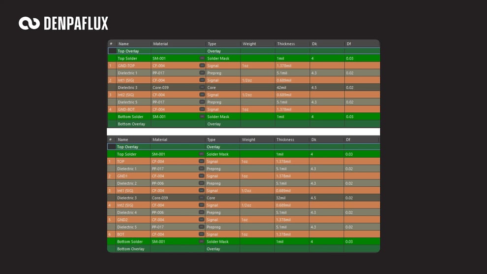
These stackups include natural shielding from the ground plane, particularly the GND/SIG/SIG/GND because it forces routing on internal layers. The GND/SIG/SIG/GND stackup can also support switching circuits, such as switching regulators, often without any performance degradation from vias connecting to the surface layer.
Changing How Circuits Are Driven
With switching circuits driving at high currents being such prominent sources of EMI, changing how circuits are driven is an excellent option for reducing EMI. There are two main ways to do this: controlling the slew rate of the driving signal, or applying spread spectrum frequency modulation. Both are covered below.
Controlling the slew rate by adjusting the driving signal edge rate is not always easy to access, partially because slew rate depends on the impedance of the load being driven. Adding series resistance is one way to easily control slew rate in a switching signal, but this can cause power to be lost and is not recommended in applications like power electronics.
Spread spectrum frequency modulation (SSFM) is one option when a driver circuit is externally controlled with a microcontroller, NCO, VCO, or is in some other way programmable. Some driver ICs implement SSFM by default and are often a preferred choice for many designers.
Chassis Bonding
Appropriate chassis bonding will allow the chassis in your enclosure to function as a shield, and this often eliminates the need for a PCB shielding cage. The appropriate bonding method depends on how power enters or leaves the system, but the goal in chassis bonding is to minimize any potential difference between the chassis and the system ground or Earth ground. This is essentially the same way metal cages are connected onto a PCB and is done to prevent capacitive coupling leading to conducted emissions.
| Ground Domain Connection | Typical Application |
| System GND to Chassis GND (direct bond) | Non-isolated DC systems, logic boards in metal enclosures |
| System GND to Chassis GND (capacitive bond) | Systems where DC isolation is needed but RF bonding is required |
| System GND to Earth GND (direct) | AC-powered equipment with Class I enclosures |
| System GND to Earth GND (through EMI filter) | AC/DC power supplies, offline converters |
| Chassis GND to Earth GND (direct bond) | Any Class I product with a conductive enclosure |
| Isolated GND to Primary GND (capacitive bridge) | Isolated DC-DC converters, galvanically isolated signal chains |
| Isolated GND to System GND (star point) | Mixed analog/digital systems with isolated measurement front-ends |
Shieldless Goes Beyond the PCB Layout
PCB-level shielding is just one option for applying shielding in a product. Other shielding methods include enclosure-level methods, such as EMI shielding gaskets, screens, or compounds. Another method that is often the cause of EMC failure is shielding along a cable, which can receive external EMI or create emissions depending on how the cable shielding is connected at each end. These points highlight how EMC is a system-level issue and is sometimes not solved in the PCB alone.
To help identify potential radiated EMI sources before they cause a test failure, look to DENPAFLUX for fast evaluation and qualification of your PCB design. We review your layout against the industry standards and regional regulations that apply to your product, then return a report that pinpoints likely EMI sources with concrete recommendations for fixing them.
How much we take on is your call. Some teams want an independent expert review to validate their direction. Others want us validating every step as they implement, with formal sign-off before each test. And some want EMC handled end to end so they can stay focused on the product. Whichever fits where you are, the same team and the same diagnostic depth sits behind your project.
See how we work or contact an expert to get started.


