
There are two very simple but very important circuits used in switching regulator topology. These circuits reduce noise, primarily by dissipating it over a resistive element. These are RC snubbers and RCD clamps, the latter sometimes also being called an RCD snubber. Most lower-power circuits and simple non-synchronous topologies can get away without these components, although they may be present in highly integrated power regulator ICs. As you get to higher powers, or when discrete components are required, that demands an RC snubber or RCD clamp circuit to control ringing on the switch node.
Where does ringing on the switch node come from? It always comes from unwanted and unintentional inductance in the connection from the switching elements, normally MOSFETs, and the switching node where an oscillating current waveform will be measured. During switching action, conduction creates large voltage fluctuations that can be measured with an oscilloscope. Because the inductance in these cases is parasitic and unavoidable, we cannot simply eliminate the inductance, and we must use one of these circuits to control ringing.
When to Use RC or RCD Snubbers
The problem we want to solve with an RC snubber or RCD clamp is the high-frequency ringing that appears on the switch node when the MOSFETs in a DC/DC converter turn on and off. This ringing is normally visible on an oscilloscope as an overshoot followed by a decaying oscillation. If the peak voltage approaches or exceeds the voltage rating of the MOSFET, diode, or controller pin, the repeated stress can reduce component lifetime or cause immediate failure. Even when the voltage is below the absolute maximum rating, the fast ringing waveform can become a strong source of conducted and radiated emissions.
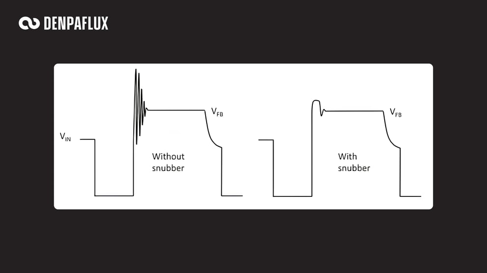 Ringing waveform in DC/DC converters with and without a snubber (RCD clamp example shown here). [Source: EEpower]
Since two different circuits are commonly proposed to solve the same problem, the designer should understand when to use each version. An RC snubber is normally used when the primary goal is damping high-frequency ringing at the switch node, across a MOSFET, across a diode, or across a rectifier in a DC/DC converter. An RCD clamp is normally used when the primary goal is limiting the peak voltage caused by leakage inductance or parasitic inductance, e.g., in switching stages where the MOSFET source-drain voltage can exceed its safety margin at turn-off.
These circuits are placed directly across or adjacent to the switching device that experiences the ringing or voltage overshoot. In a typical DC/DC converter, an RC snubber can be connected from the switch node to the local power return, across the MOSFET drain and source, or across a diode or rectifier that produces the ringing waveform. An RCD clamp is normally connected so that the diode conducts only when the switch-node or drain voltage exceeds the clamp threshold, charging the clamp capacitor and then allowing the resistor to dissipate the captured energy.
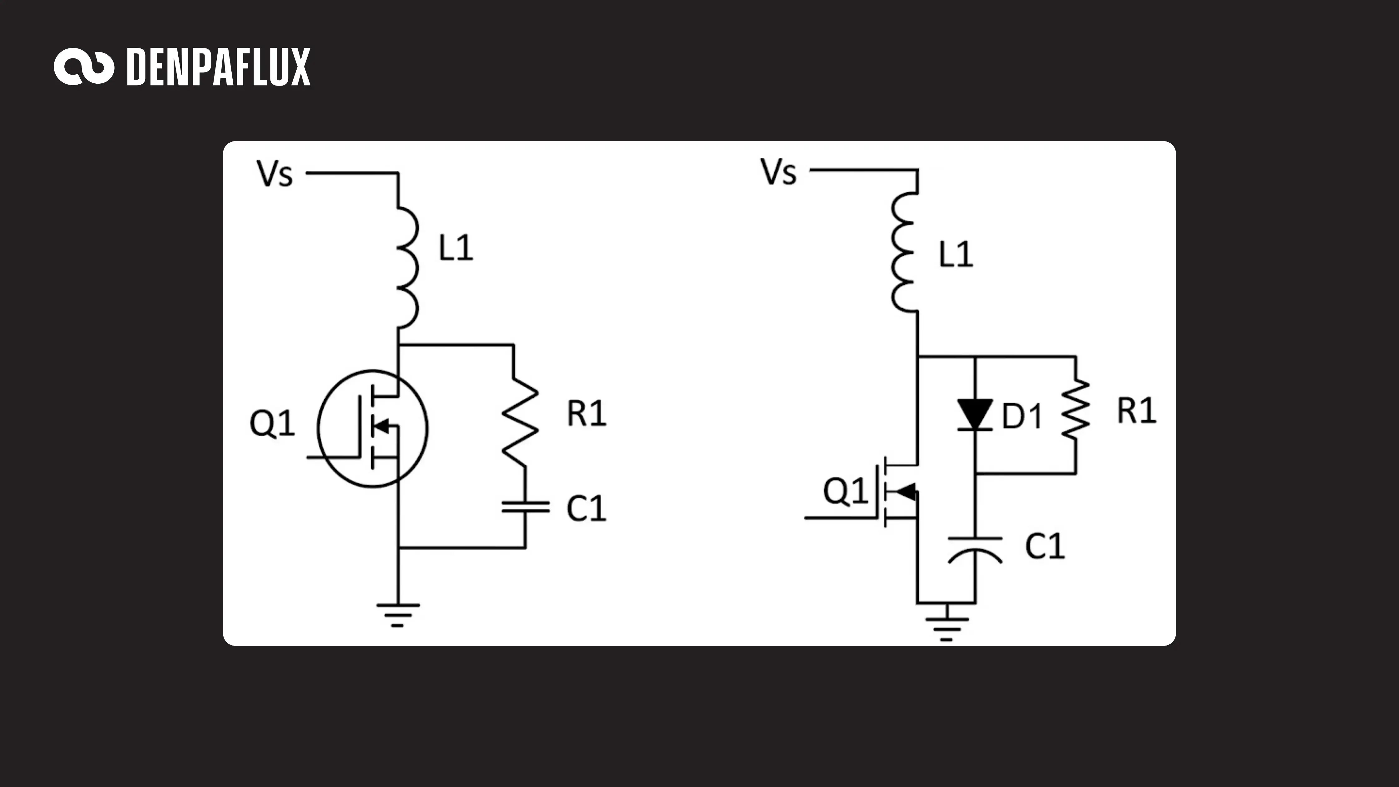 Left: RC snubber circuit; Right: RCD clamp circuit
Both circuits dissipate the energy associated with ringing instead of allowing it to continue oscillating between parasitic inductance and capacitance. In an RC snubber, the capacitor provides a short high-frequency current path, and the resistor dissipates the ringing energy as heat while damping the oscillation. In an RCD clamp, the diode conducts during the voltage overshoot event and routes energy into the clamp capacitor. The resistor then bleeds charge from the capacitor between switching cycles, while the diode prevents the capacitor from discharging back into the switch node during normal operation.
RC Snubber Design
An RC snubber is normally designed after taking measurements of the ringing waveform at the switch node in order to determine the total parasitic capacitance (in excess of the MOSFET internal capacitances). Then add a known test capacitor from the ringing node to the local return and measure the new ringing frequency. This gives an estimate of the parasitic capacitance and inductance that are producing the ringing.
A simple measurement-based method is:
Cp = Ctest / [(fr1/fr2 )2 - 1]
Lp = 1 / [(2πfr1 )2 Cp]
Once the parasitic capacitance Cp and parasitic inductance Lp are known, choose a snubber capacitance that is large enough to dominate the parasitic capacitance but not so large that it creates excessive loss. A typical starting point is:
Cs = 2Cp to 4Cp
The resistor is then selected to approximately match the impedance of the ringing network:
Rs ≈ √(Lp/Cs)
The final resistor value should be adjusted while observing the oscilloscope waveform and checking that the ringing becomes reasonably damped. As a final check, calculate the power dissipated across the resistor to ensure the component does not fail.
RCD Clamp Design
An RCD clamp is typically placed on the primary side of a transformer/coupled inductor and will depend on the leakage inductance of the inductive element. The leakage inductance can be measured with an LCR meter. We first define the maximum voltage that the switching device is allowed to see (less than a FET's rated voltage, for example).
The clamp should not conduct during normal switching action; it should conduct only when leakage inductance or parasitic inductance forces the drain or switch-node voltage above the desired limit.
The energy that must be absorbed is commonly estimated from the measured leakage inductance that causes the overshoot:
E = ½LI2pk
where L is the leakage or parasitic inductance and Ipk is the peak current at the instant the switch turns off. The average power dissipated in the clamp is then:
Pclamp = Efsw
where fsw is the switching frequency.
Next, choose the clamp capacitor voltage VC. This is the voltage that appears across the clamp capacitor and resistor during clamp action. The resistor is selected so that it dissipates the captured energy between switching events:
R = V2c / Pclamp
The capacitor is determined based on the allowable clamp voltage ripple, which can be chosen by the designer. A typical goal is ~5% ripple, and a useful estimate is:
C ≥ E/(RΔV)
A larger capacitor reduces ripple and produces a more stable clamp voltage, but it can also increase turn-on stress if the clamp is not allowed to discharge properly through the resistor. The diode should be a fast-recovery or Schottky diode with adequate reverse-voltage rating, current rating, and reverse recovery time. Its job is to conduct only during the overshoot event, charge the clamp capacitor quickly, and then block reverse current during the rest of the switching cycle.
Snubber/Clamp Placement
The ideal place to put these circuits is close to the node where the ringing voltage is measured. Ideally, it will be a direct connection between the node and the input voltage/ground, depending on topology. This is because it reduces the current loop area associated with the ringing voltage, and this will reduce radiated emissions associated with residual ringing.
PCB layout for power electronics can look simple, since there are often no high-speed digital protocols or RF interconnects, but these systems carry real EMI risk. DENPAFLUX helps designers analyze their PCB and system design to identify those risks. We review your layout against the industry standards and regional regulations that apply to your product, then return a report that pinpoints likely EMI sources with concrete recommendations for fixing them.
How much we take on is your call. Some teams want an independent expert review to validate their direction. Others want us validating every step as they implement, with formal sign-off before each test. And some want EMC handled end to end so they can stay focused on the product. Whichever fits where you are, the same team and the same diagnostic depth sits behind your project.
.png?width=352&name=Why%20_70%25%20of%20HV%20Products%20Fail%20EMC%20the%20First%20Time%20(2).png)
.png?width=352&name=EMC%20basics%20for%20SiC_GaN%20switching%20-%20What%20changed%20vs.%20IGBT%20(2).png)